Previously in the posts, GDT was the topic and the Wikipedia article with the code snippet was basically setting up kernel code segment and kernel data segment for paging. Remember the granularity flag, this was set to units of paging or in other words, set to 1. Let’s get into paging for this blog. It is highly relevant to the capstone, as the team is implementing a paging scheme within the final product, the Minimalistic OS.
As a reminder, both segment and paging are types of memory management methods. The virtual memory is actually a label to call a memory process of which the RAM/physical/main memory works together with a secondary storage device, such as a hard disk. More details about this virtual memory — later!
Sort of? Paging is a way to make the individual processes running feel like they are the only ones running on the disk. Much like a book, the reader is fixed on all the information contained on one page, then continued to the next page, however still solely focused on the page at hand. Another book related perspective could be that the author has their whole masterpiece on a continuous paper spool. To make a book, the spool is divided into equal sized chunks (pages) and stitched together to make a book.
With paging, a very nice and convenient sequenced logical memory space is provided for each of the programs. This is usually 4KB chunks or pages. However, this is all an illusion, as these individual processes are not actually alone, they are joined by others who also take part into this grand illusion, known as paging. Continuous memory allocation is what the individual processes will be using within the logical memory space probably is not continuous (or at least has the option of not having to be) within the physical memory space, in fact, this was a main driver for the creation of paging memory management.
created in pptx
Paging will require a type of look-up table or what is known as the page table, which holds all the pages. This table will be pointed to from a paging directory entry. In this table the logical address (the one the illusion-ed individual process will be using) will be mapped to an actual, no illusion, physical memory address or if using virtual memory scheme then, there is a possibility the mapping will be to a special place within a hard disk or the like. However, even if using a virtual memory scheme or not, the page table will map the illusion logical memory to a physical place in memory.
Let us first start off with some chunk located in the logical address space. This logical address will have two pieces to its address: selector and offset. The selector will be used to point to something handy in the descriptor table, of which will be the particular segment descriptor. The offset will be used with the segment descriptor to create the linear address. The linear address contains the page directory entry, page table entry, and the offset within the physical address hosting the page frame.
Virtual Memory Purpose
Virtual memory was originally thought to help out the limitations of a RAM/main memory size. As stated before, the virtual memory scheme is a usage between the RAM/main memory and a secondary storage device, such as a hard drive. The RAM/main memory will accumulate memory chunks (pages), with an allocated size, all the same for paging granularity, then begin moving the unused memory chunks (pages) into a designated storage place within this secondary memory device. In a sense, the virtual memory scheme creates another illusion of a huge and ample space “main memory”. However, in reality, this actually is far from the case.
We have all these unused pages/memory chunks within the secondary storage device waiting, once they are needed, they are placed back to the RAM/main memory place. The page table is consistently working to keep track of all these memory chunks. It can be a daunting task, surely!
Troublesome Paging
Disk thrashing and fragmented processes are the main issues with the use of paging. If you were to use segmentation memory management these are not issues, however with segmentation you are not using every last available memory space and memory fragmentation effects will be seen soon. Trade offs.
Disk thrashing limits application-level processing by page faults and over worked virtual memory abilities. It is data swapping at its limits! The moving of data does not allow for effective storage in the physical memory.
fragmented processes are processes which really don’t have all that they need to carry out their purpose. This becomes present when the hosting of the data paging is not adequate enough to piece all together during the use of a process from physical memory.
Best to decided what is the goal of your system — utilize main memory effectively (paging) or aim for fast access by processor (segmentation). Modern systems tend towards paging and a hybrid of the two types.
Now our team is focused on the protected mode learning and building. A great binary data structure used by the x86 Intel processors is the Global Descriptor Table (GDT). Think of it like a barcode. With any data structure its means are to provide a usage framework, and for the GDT, this framework created generally includes memory areas or segments described. For this week’s blog the goal will be to explain the Wikipedia Netwide Assembler (nasm) assembly language implementation of a generic GDT which opens up all 4GB of memory to a usable state. This code is free and accessible, therefore it also could entice the reader to go down the various rabbit holes during a visit, as wiki is never in short supply!
Nope. You do not actually need to make one of these IF you are using a bootloader mechanism which will do this type of work for you, i.e. GRUB. And… if you were to utilize GRUB and become determined to create your own GDT within, as in write over the already-there-GDT, a “triple fault” will occur and the computing machine will reset. Sad day!
However IF you are not using a bootloader mechanism and aim to have memory protection once your OS is initialize, yes, and emphatic YES! Unless you are making something uber special and some how do not need GDT for paging mechanism or similar.
Courtesy of giphy
What?!? — x86 segment descriptor?
It shall be noted, the GDT data structure can do more than describe memory chunks/segments, however these extra things are not needed for our project at the moment, therefore detailed dives into all the possibilities of a GDT data structure will not be commenced here.
Segment descriptors are used by the x86 architectures as a way for translating a logical address to a linear address — the segment descriptors are here to describe the memory segment assigned within the logical address. Linear address is a virtual address, an address where a thing lives from the understanding of the executing environment. The linear address does not actually have to be a physical address, especially in the realm of virtual memory usage, which is applicable here. You can think of this as a form of address “normalization”.
Segment descriptors will contain at least the following:
Base Address
Segment Size/Limit
Access/Privilege Rights (think memory protection!)
Flags
created in pptxcreate in pptx
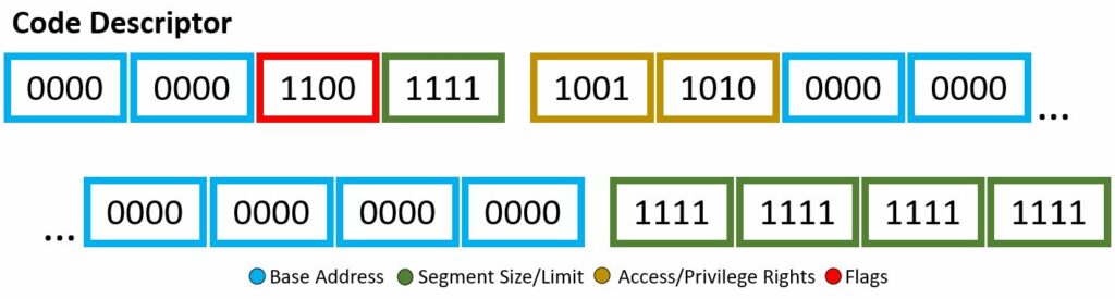
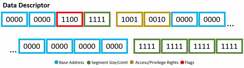
Through the descriptor framework we can make things, such as the code descriptor and data descriptor, shown above. These examples will also be a visual for the bits used within the Wikipedia code snippet to be explained.
In our code example, soon to be explained with a fine-toothed comb, there are two segment descriptor data structure implementations: code and data. I mean if you count the “dummy” one full of 0’s, then i guess we actually have three. Each will have different bit set-up, however still based off the four attributes listed above. You may note, the scheme of which bits are associated with which attribute are not exactly… orderly, there are a few jumps around and continuing — however, all will be explained!
Base Address
This is your 32-bit linear address, where we are stating the starting of the memory segment. If your architecture is 64-bit based, this is ignored.
Segment Size/Limit
This is your 20-bit value, where we are stating the maximum allowable addressing unit. This could be 1 byte units or 4 KB units. Here, you just want to place the address of the last accessible data place + 1. If your architecture is 64-bit based, this is ignored.
Access/Privilege Rights
This is your 8-bit value, where you highlight description of access. Four bits describe the presence of the segment, ring level of privilege, type of descriptor. The other four bits describes the type.
[ P . DPL . DPL . DT . Type . C|E . R|W . A]
P – segment presence. If the bit value is 0 then an exception will be given if referred to this segment and if the bit value is 1, then no exception will be given if segment is referred to.
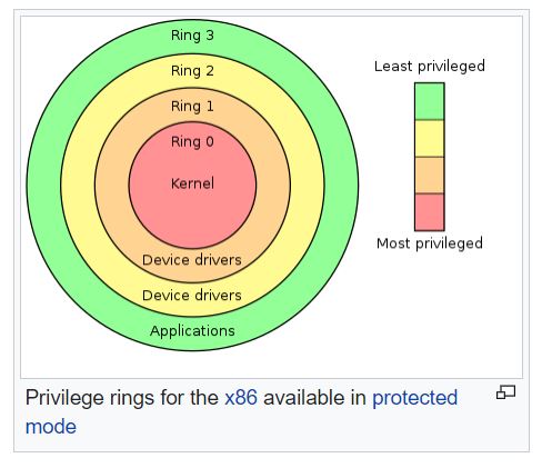
DPL – (two bits) – Descriptor privilege level field or ring level to access this descriptor. Two bits allows binary-11 or decimal-3, up to ring 3. The graphic below depicts the ring level meanings and usual privilege-based assigned.
Courtesy of Wikipedia
DT – literally a fixed one, descriptor type, this is a descriptor, must be one.
Type – This is a huge switch. If this value is 0, then descriptor is a data segment and if the value is 1 then the descriptor is a code segment. You will see the underlying other bits which base off this set/not set of a bit. For stack/data segments use of E, R, and flag D. For code segment use of C, W, and flag B.
[C or E] E – Expanded-down or direction bit. (type – 0) meaning if the bit is 1 then the segment will grow in a downward fashion, while a bit of 0 will grow up, the offset will be less than the limit. C – Conforming bit. (type – 1) meaning is the bit value is 1 then the code can be executed from less=privileges levels and if the bit value is 0, then the code segment can only be access by this ring and above.
[R or W] R – Readable bit. Not to use with code segments (type – 1). (type – 0) read access is not abled when set to 0 and read access is abled when set to 1. W – Writeable bit. Not to use with data segments (type – 0). (type – 1) write access is not abled when set to 0 and write access is abled when set to 1.
A – Set to 1 by hardware/CPU when segment is accessed and set to 0 by software.
Flags
This is your 4-bit value, where you describe the granularity, operand size, and availability for the system.
[ G . D|B . L . AVL ]
G – granularity this is tied closely for paging work. If the value at this bit is 0, then units of bytes are utilized (max 2^20 bytes) known as byte granularity and if the bit value is set or 1, then unites of 4096-byte pages (max 2^32 bytes) known as paging granularity.
[D or B] D – Default operand size. If the value of the bit is 0 then it is 16-bit max 0x0000FFFF and if the value is 1 then 32-bit segment. B – Big operand size. If the value of the bit is 0, same as D and if the value is 1 then the maximum offset size for the data segment is 32-bit 0xFFFFFFFF.
L – long-mode flag, ability to use 64-bit segment rules. If the value is 0 then not-64-bit and if the value is 1 then 64-bit applies (D must be set to 0 for proper usage).
AVL – Available for software use, not utilized for hardware, it is like a wildcard flag you could use within your program or a reserved flag.
Example of GDT
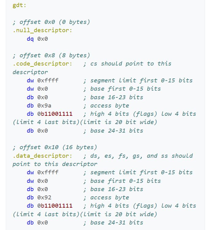
Below you will view the nasm assembly code for a simple gdt. After the photo, we will dive into what all this means.
Courtesy of Wikipedia
Two things to point out here in this photo. First, the access bytes would have been more helpful to the reader if these were given in binary, rather than hexadecimal (‘0x9a’ and ‘0x92’). Secord, the assembler does not have something lower in amount of bits than ‘db’, which is 8-bit direct bits. If it did, it could help the reader better understand the separation that is actually going on within the ‘0b11001111’ and ‘0b11001111’, where we are forced to combine the flag bits with a portion of the limit bits.
I hope by reading this code you would agree the jumping and disorderly placement of bit meaning for these descriptors. However, this is probably due to the historical or general hardware ease of interpretation with the ending machine code after the assembler helps out.
Now, where is my comb?
We are establishing three different segments: null, kernel mode code, and kernel mode data. There is no user space in this or the task state segment (TSS), of which are common frameworks one would set up for a minimalistic OS. Mainly for the user code and user data the ring would be three instead of zero. For the TSS, the ring would be one. I digress. In this code snippet, the aim is to open up and access 4 GB, 0x0000000 to 0xFFFFFFFF. Therefore, the base address will be 0x00000000 and the limit will be (0xFFFFFFFF – 0x00000000) + 1, or 0xFFFFFFFF. You will see the use of the flags for this large of a limit.
The null descriptor segment is used by the CPU only and should not have any data in there. The Boch emulator will give a limit exception if you did not set one of these up. Since the null descriptor is 8 bytes, it could be used for the pointer to the GDT, which is 6 bytes. However, in this example all the bytes and bits are set to 0.
created in pptx
The 8 byte kernel mode code descriptor segment has the following:
Therefore, to build out this segment descriptor, we use the scheme within the pptx diagram above. To speak on the access rights of 0x9a or b1001 1010 in detail, let’s begin. The segment presence is set, therefore no exception shall be expected when referring this segment. The two-bit DPL is 00, therefore this code descriptor has ring-0 or highest privileges. Makes sense, you don’t want malicious programs or blissfully unaware users to take advantage of the kernel code descriptor. The DT is set, obvious, as this is indeed a descriptor. The type is given as set or announcing this is a code segment, meaning the use of C, W, and flag B. The conforming bit is not set, therefore this code segment can only be accessed by its own privilege ring and higher (however in this case, it is already the highest level of privilege). The writable bit is set, therefore write access is granted. Finally, the Access bit is not set, therefore it is currently in software’s hands. This final bit being not set is a little odd, generally you want to keep this not set and let the hardware have its turn. Oh well, this is Wikipedia code snippets… As for the flags, b1100, there is more to uncover. The granularity bit is set, therefore paging units are being utilized. The operand size is set, meaning because the type was set in the access bytes, we are granted to use the big opcode size, of which if set, which it is, the the maximum offset size for the data segment is 32-bit 0xFFFFFFFF. This is allowing us to be able to reach the actual desired limit. The long-mode flag is not set, therefore 64-bit rules will not be applied. Lastly, the AVL or wildcard flag is not set or being used.
created in pptx
The 8 byte kernel mode data descriptor segment has the following:
You might notice, wow this is very similar to the code segment descriptor — right you are. It seems whoever put this code snippet together wanted the only different between the two, well, very slim. Nevertheless, lets dive into it. The access bits of b1001 0010 will be our first subject. The segment presence bit is set, no exception will be given if this code segment is referenced. The DPL two-bits are set to 00, of which is ring-0, highest privilege. The DT is set, well yes, this is a descriptor! The type given is not set, therefore it is a stack/data segment type. The use of E, R, and D-flag will be applied. The Expanded-down or direction bit is not set, therefore augmentation will begin upward, in other words the offset will be greater than the limit. The readable bit is set, read access is enabled. Once again, the access is set to software, and still questionable, the reading in other resources state this should actually be left to 1 as the CPU/hardware will be accessing it. Now for the flag byte, b1100. The granularity bit is set, therefore units of paging will be utilized. We had type 0, therefore the default operand size will be used. This default operand size bit is set, meaning 32-bit segment rules. The long-mode flag is not set, no use of 64-bit rules and the wild card or AVL bit is not set meaning this is not used either.
From the code snippet, their comments show the offsets between the different descriptor segments is 8-bytes. This will be important and handy when using these in the actual initialization of the kernel file.
Now we have this GDT descriptor, what next?
Meet opcode lgdt !
During the initial kernel set up, we are tasked with setting up the segment registers, of which we need this framework to be described. Who better to ask for a description of descriptors than our GDT? We will call this opcode along with the value we will be storing at a pointer to the GDT descriptor, another framework. Man! We will now be embedded our GDT framework into a GDT descriptor framework. The GDT Descriptor will hold the offset (linear address) and the size of the GDT. Bam! Now we have connected things and can start adding entries of code and data segments.
This week’s topic will be discussing NAND hardware. This relates to the Capstone building of a minimalistic OS, as within the level of hardware, you will find these lurking in many board areas. Maybe lurking is an odd word to use, the NAND gates have no intension of attack, much like their inputs, they are actually quite the opposite. Early in the program here at OSU, I remember there was a statement read somewhere about how a computer has the potential to be fully utilized with pure NAND gate logic. Thinking at the time oh, that is cool, okay thanks for the fun fact. Now, many courses later and independent exploring, this seems like a fascinating statement. To the interwebs! Okay, I’m back. Found a blog from a person who actually did just that, created a computer fully based on NAND chips, below you will find it in operation and here is a link to this person’s blog.
courtesy of YouTube
Here is a photo with some of the boards fully of only NAND chips, please visit this person’s blog listed above for more information and photos, including this one.
The NAND chips you viewed in the photograph above are packaged die chips, they have a protective covering over a tiny chip, this chip has connection wiring to each of the pins. It shall also be noted, a single chip can and probably has multiple gates within it. The logic for the gates also does not have to be limited to only two inputs, as most internet representations will try to persuade you. In fact, you could have say eight inputs and one output or have one input split into a two-input place with a single output or other combos. Quick note, the last option listed is called an inverter or a NOT gate. With the possibilities of a NAND gate, it is considered to be functionally complete or a universal gate, just like a NOR gate. This bold statements means NAND gates alone have the ability to create any other logic function, hence the NANDputer possibility — and creation.
CMOS vs. TTL NAND Gates
Let us get the acronyms out of the way. CMOS stands for Complementary Metal Oxide Semiconductor and TTL stands for Transistor Transistor Logic. One more used later is MOSFET which stands for Metal Oxide Semiconductor Field Effect Transistor. “Metal Oxide Semiconductor” means the gate electrode is placed on an oxide insulator and this oxide insulator is on top of a semiconductor material. It is a fancy label for the stacking of materials. In the 1970s metal was actually used as the gate, however it has moved towards a non-metal medium — however we still use this term. These are very wordy, the rest of the blog will be using the acronyms. Most comparative reasoning will boil down to cost, however this will not be the focus of the comparison listed about these NAND gates. Below you will also see the inner-workings schematics of both types of NAND gates.
CMOS
CMOS actually has a combination of types, complementing each other, the NMOS and PMOS MOSFETs. The Bell Laboratory colleagues, Dawon Kahng and Mohamed Atalla, were responsible for the invention of the MOSFET. MOSFETS will have at least three terminals: source (could have multiple), gate, and drain. The movement of current between the drain and source is controlled by the voltage at the gate. For NMOS, the source/drain terminals are made of n-type semiconductors, while PMOS has the source/drain terminals made of p-type semiconductors/substrates.
But what are n-type and p-type semiconductors/substrates?
This labeling system all has to do with the impurities added to the pure silicon/germanium structure. P-type will have an additive with three-valence electrons, while n-type will have five-valence electrons. The silicon or germanium or other material lattice will have four-valence electrons. Therefore if the p-type or n-type additives are applied will either have create a “hole” where the electrons can jump about, filling each of the open places as seen in p-type, while n-type will have an extra electron randomly bouncing with no where to call home, it is far out from the nucleus of the additive, therefore its ties are not too great and the exploration can happen. Quick note on the additives, you could be surprised! P-type will have additives of elements with three-valence electrons, such as: aluminum, gallium, indium, and thallium. N-type will have additives of elements with five-valence electrons, such as: phosphorous, arsenic, antimony, and bismuth.
Now… back to the CMOS topic.
The CMOS process was created by a team of EEs at Fairchild Semiconductor Corporation, “Tom” Sah and Frank Wanlass. This process, the Complementary MOS establishes a clear path to output as the source of power (1) or ground (0). The power source paths mush be in complement to all the paths to ground. Meaning, the PMOS (p-type) transistors in parallel have corresponding NMOS (n-type) transistors in series, while the PMOS transistors in series have a corresponding NMOS transistor in parallel.
Here are some comments about the generalities of using a CMOS. CMOS uses little power for its NAND IC, making them the more preferred in practice and within products. The amount of time it takes for a signal to be received within a CMOS NAND IC is between 20-50nS. CMOS will require voltage levels 2/3 given power. CMOS is more sensitive to electromagnetic disruptions. More noise reduction can be found within CMOS. You can fit more logic within a given space using CMOS.
TTL
The original name for TTL was actually TCTL or Transistor Coupled Transistor Logic. I know, the statement above mentioned acronym would all be defined there, well, here is one more, I may add another later in the blog too. In 1961, EE James Buie of Thompson-Ramo-Woolridge Inc., invented the first TTL. A TTL NAND gate will have a bipolar (2 options) transistor with emitters as inputs, whose output will be buffered by an amplifier. Another acronym to have, BJT, stands for bipolar junction transistor. This is the grand name this logic has utilized too. Today, Texas Instruments has continued to have the standard for TTL IC chips manufacturing for usage, especially their 7400 NAND gate series.
Here are some comments about the generalities of using a TTL. The amount of time it takes for a signal to be received within a TTL NAND IC is 10nS. TTL will require voltage levels between 4.75 to 5.25 V. TTL is less sensitive to electromagnetic disruptions. Less noise reduction can be found within TTL. You can fit less logic within a given space using TTL. Some efforts have been made with creating chips which use less power than the original TTL design.
Visual Comparison
Interestingly, the CMOS will be the ultimate choice, however TTL will still be used as “glue logic” or parts of the circuitry for integration between integrated circuits (ICs). Another interesting fact to note, when the shift became apparent to move towards CMOS ICs, the manufacturers would create a chip with pins identical to layout of the TTL, for “easy” upgrades.
CMOS NAND gateTTL NAND gateCourtesy of leanabout-electronics
This diagram above shows the inner-workings of the CMOS and TTL. You can visually see the p-type and n-type MOS, which have the three: source, gate, and drain within the CMOS diagram. You can also see the complementary structure it holds between the p-type and n-type MOSFETs. The TTL shows the bubble label as the transistors. T1 in the diagram is the bi-polar possible entries or inputs, you can see the two options. The other transistors (T2, T3, T4) are used as an amplifier. Hopefully seeing the two visuals together will aide with solidifying the subjects spoke on within this post.
Since the capstone will be about building a minimalistic operating system, a great starting place to investigate would be, what is there before we have the OS? If this is TLDR; go to end of blog for a nice process diagram with the important parts.
Content Sources
wikipedia
Intel Software Developer Manual Vol. I Chapter 3
Rootkits and Bootkits [ISBN: 978-1-59327-716-1]
Upgrading and Repairing PCs [ISBN: 978-0-7897-5610-7]
Toto, I have a feeling we are not in Kansas anymore…
Before all ability to have an OS loaded and functioning, we are existing in a strange and peculiar place. This place is known as the CPU in real mode place. This real mode is a space, even before BIOS installation happens, it is like the air in the space. The original CPU chips would be in 16-bit register usage, which is what this mode is. You might be wondering why this is the case. For one note, Intel aimed at always being “backward compatible”, meaning even if the CPU was upgraded, legacy os/software could still be able to perform. Secondly, when we have the 16-bit real mode as the original start, it is not quite like the original 16-bit normal mode one could see back when these chips were the top-tech, as this had a huge flaw of critical memory being able to be handled by the general user — now, more steps have been in place to still give the 16-bit environment, with more security. The need of the OS can change this mode with a single line within their source code, however initially the state will be 16-bit.
courtesy of giphy.com
Second part of growing the ecosystem within this space would be this installation of BIOS. BIOS is a way to have “bare bones” access to in and out devices, hence the name Basic Input Output System. How does the bare system even have loading capabilities to a BIOS? It is a chip, usually an EEROM chip. Fun fact, some earlier BIOS chips would have a window you could look inside, not the exact aim here. I mean it is always interesting to view the die’s internals, however there is another reason why this little window was here. Oh, no, it is also not the case either as a tribute to Windows OS as literally having a window. These little windows were for erasing with a UV light beam. There was a phase of chips created of which you could erase by UV light waves. Hoped you liked the fun fact, back to BIOS. You can make a connection between the ROM cartridges (think BIOS) for a NES system (think CPU), they have the game, and you already have base instruction set on what to do, if asked. BIOS is like another layer of interaction we can have to hardware, at the very start of the power up.
More on BIOS
First BIOS was created in 1974, developer Gary Kildall, for the CP/M operating system, produced in 1975 for IBM PC. His aim for BIOS literally was the sole piece of the system which loads to communicate with machine hardware. Today, most BIOS are installed within the motherboards of the whole system or some other type of adapter-like concept, like adapter boards. Companies which are used by most Western technology manufacturers include: American Megatrends, Inc. [AMI], Awards Software, Insyde Software, and Phoenix Technologies (owns Awards Software). There have been advances to make more efficient BIOS implementations for each particular purpose. The purposes could be for pcs, servers, mobile phones, USB devices, and also ones optimized for 32-bit or 64-bit needs, plus more! The Unified Extensible Firmware Interface (UEFI) is usually weaved into the BIOS, for needs of handling OS loading from hard drives with partitions larger than 2TB, all listed companies work within these product needs too.
That is all great, what about more details about BIOS capabilities?
BIOS has subroutines of which act as interrupt procedures. Each will have its own needed loaded parameters (or not) in particular registers before calling. Below is a list from Wikipedia.
int 0x05 -- detects bound failure
int 0x08 -- real time clock (18.2 times/sec)
         -- increments time-of-day counter with
int 0x09 -- keyboard interrupt
int 0x10 -- video/display services (write something, teletype, etc.)
int 0x11 -- returns equipment list
int 0x12 -- returns base memory list (first 640 KB)
int 0x13 -- low level disk services
         -- (read/write/get/set/extend/eject/etc.)
int 0x14 -- serial port servies
int 0x15 -- miscellaneous system services
int 0x16 -- keyboard input/storing services
int 0x17 -- printer services
int 0x18 -- execute Cassette BASIC,
         -- modern,  will boot from a network
         -- modern, bootloader has failed at some task
int 0x19 -- used to load the OS
int 0x1A -- real time clock services and PCI servies
int 0x1B -- ctlr-break handler, called by int 0x09
int 0x1C -- timer tick handler, called by int 0x08
int 0x1D -- points to VPT (Video Parameter Table) holding video modes
int 0x1E -- points to DPT (Diskette Parameter Table)
         -- info on diskettes
int 0x1F -- points to VGCT (Video Graphics Character Table)
         -- ASCII characters
int 0x41 -- address pointer first hard drive
int 0x42 -- address pointer second hard drive
int 0x4A -- called by RTC for alarm
MBR Notes
Master Boot Record or MBR, is the place on the chip memory where the system vector is stored. You can think of this as a controller between the incoming exceptions and what next to do with forwarding to proper handlers. It should be noted here this data structure will not be erased during a firmware update, it is here to stay with this chip for the long haul, like a dear friend. Ultimately, this provides information on boot code and hard drive partitions within the whole system. Below is a nice comparison of MBR compositions. Capacity will always be 512 bytes on all, as you will note.
Classic MBRModern MBRcourtesy of Wikipedia
Main task of MBR is to determine the active partitions of bootable hard drive — this holds the OS to load. When the game of hide and seek is over, the MBR reads and executes the boot code. Here is the data struct for a MBR:
The BootCode with memory location is where the boot code exists, and the mbrSignature is the Magic Number or pattern, depending on if you check out the binary equivalent to 0xAA55. The internet will tell this is a nice pattern which was originally used for detection of errors within connecting devices. It probably is an easy pattern for the machine level parsing to pick up too. Something to note, this probably should have been placed earlier in the paragraph, the [0x1BE] is not the 512 bytes, it is actually 446 bytes, meaning that this is the maximum allotted space the boot code is allowed to have, as the other bytes between must be used for other useful things.
MBR Notes – Partition Table
This is the part within the above MASTER_BOOT_RECORD structure will be parsing, and like above states, it has four parts.
(1) Partition status will let the system know if this is the single active partition or not, it is another. (2) Partition types will be something similar to EXTENDED MBR, FAT12, FAT16, FAT32, IFS, LDM, NTFS, etc. Oh, if the type is labeled as ‘0’, this means it is unused. The MBR is not granted the ability to parse the particular file systems, so it will read and execute the first sector of the partition, known as VBR — houses other things, more on that later. (3) Partition lbsStart and (4) partition size will tell exactly the location of the partition on the disk, represented in sectors. For a floppy, for example, it could be given in the CSH (cylinder-sector-head) format, think about the organization of the platters!
VBR Notes
This is the first sector of the partition and readable by the MBR. Here you will find BIOS parameter block, bootstrap code. The layout of these will always be dependent of the filesystem structure of the main partition. Mainly, the VBR will load the IPL or initial program loader, BIOS parameter block is held here, text strings for human readable/printable error alerts, and Magic Number 0xAA55 as a signature.
VBR Notes – IPL
This Initial Program Loader will read and load the OS boot manager from the file system. Once this happens, the boot manager (windows) or boot loader will fully take over.
Putting it all together
Even though this listing will not be of today’s steps, the idea essentially remains the same. Having a step through outline on a process is usually helpful to solidify what is actually happening, which is why it is here for your viewing pleasure.
Legacy Boot Process Steps [1980s-2000s]
Cold Boot — power is connected/on
Power supply testing
ROM BIOS execution
ROM BIOS hardware testing
Video testing
Memory testing
Power-On Self-Test (POST) — full hardware test, skipped if warm/soft boot
MBR testing at defaulted first sector of boot drive, stated within the BIOS setup schema
MBR execution
OS file initialization
Base device driver initialization
device status check
configuration file reading
command shell loading
Startup command file execution of shell
Previously, one can note, a lot of care went into ensuring each piece of equipment was fully functioning enough to go to the next step in the sequence, a good idea.
Conclusion
Below is a high-level overview of all the topics briefly covered within this post, outlining what is to be expected in the states preceding the Minimalistic OS fully running and speaking directly to the hardware.
process diagram of the needs before actually fully running the new OS (created in ms paint)
So the question remains, and will not be answered in this blog or a future post — is it possible to have the OS as a chip directly on the motherboard and skip all the steps of the BIOS interactions with hardware scheme. Can you have the OS as the starting point, and if you can, could this type of setup prevent more low level attacks from the venerable starting in the magic and spacey boot land?